Abstract
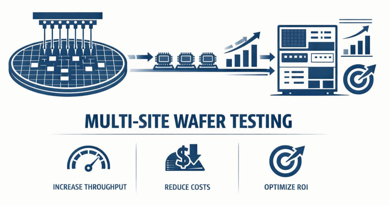
Multi-site wafer testing is a fundamental technique in high-volume semiconductor manufacturing that enables simultaneous electrical characterization of multiple dies on a single wafer in one prober touchdown. By testing N devices under test (DUTs) in parallel, manufacturers improve throughput, reduce cost-of-test (CoT), and increase utilization of expensive Automated Test Equipment (ATE) [1].
This document provides a comprehensive, technically rigorous examination of multi-site wafer testing, including economic drivers, system-level architecture, engineering challenges, mitigation strategies, throughput and efficiency modeling, failure modes, test-program architecture with pseudocode, advanced probe-card technologies, AI-assisted optimization, and representative industrial case studies. The material is intended for test engineers, probe-card designers, and engineering managers responsible for deploying and optimizing multi-site test strategies.
1. Introduction
1.1 Economic Motivation and Technical Objective
Semiconductor test is a cost-critical stage under sustained pressure. Advanced-node devices (5 nm, 3 nm, and below) contain very high transistor density in compact, thermally dense, and electrically complex dies. A single high-speed functional flow can require hundreds of seconds of ATE time per device. When scaled across full wafer and lot volumes, single-site testing can make test cost per die economically prohibitive.
Multi-site wafer probing addresses this constraint by contacting and testing N dies simultaneously per touchdown. Effective throughput approaches N × T_single⁻¹ DUTs/second, amortizing fixed overhead (prober stepping, deskew, and power settling) across all active sites. A single ATE platform can therefore support substantially higher output without proportional increases in floor space or staffing.
The objective of this document is to provide a quantitative framework for understanding how multi-site testing delivers cost benefit, which engineering disciplines constrain that benefit, and how to measure, model, and improve parallelism efficiency (η) from bring-up through production maturity.
1.2 The Cost-of-Test Equation
The fundamental per-die cost model for wafer sort is:
CoT ($/die) = (Tester Depreciation + Prober Cost + Overhead)
             ─────────────────────────────────────────────────
              Throughput [DUTs/h] × Utilization
Increasing site count N raises throughput proportionally (modulo efficiency losses), while depreciation and overhead remain essentially fixed. For a site count of N with parallelism efficiency η:
Effective Throughput = N × η × (1 / T_single)   [DUTs / second]

Where:
  N          = number of simultaneous sites
  η ∈ (0,1]  = parallelism efficiency
  T_single   = single-site test time [seconds]
Achieving high η is the principal engineering challenge of multi-site testing. This document systematically examines the factors that limit η and the strategies to maximize it.
1.3 Advanced-Node Challenges
Advanced CMOS nodes compound each challenge. Higher operating frequencies tighten skew budgets; lower supply voltages (0.7–1.0 V) reduce IR-drop tolerance; leakage currents scale with area, worsening thermal non-uniformity; and higher pin counts demand larger probe cards with more complex routing. These trends make disciplined multi-site engineering more—not less—important as device generations advance.
1.4 Scope of This Document
This document covers multi-site wafer-probe testing exclusively. Although some concepts (resource partitioning, synchronization) apply equally to package-level testing, the unique constraints of wafer probing—probe card mechanics, chuck temperature control, prober stepping, and die-level granularity—receive dedicated treatment.
Key Takeaways
- Multi-site testing amortizes fixed test overhead across N sites, reducing CoT by up to 1/N in the ideal case.
- Parallelism efficiency η captures all losses; maximizing η is the core engineering objective.
- Advanced nodes increase every challenge: skew budgets tighten, IR-drop tolerance shrinks, probe cards grow in complexity.
- This document provides quantitative frameworks and pseudocode to measure and improve η in production.
Before examining each engineering challenge in depth, §2 provides an overview of all major challenge domains so readers can understand how they interrelate before diving into detail.
2. Engineering Challenges Overview
Multi-site testing is not a linear extension of single-site testing. Each additional site introduces non-linear coupling effects across electrical, mechanical, and thermal domains. Understanding how these challenges interact is the first step toward systematic mitigation.
Each node influences every other; co-design is critical.
| ID | Challenge | Root Cause | Primary Impact | Section |
|---|---|---|---|---|
| C1 | Timing skew | Trace-length mismatch, temperature gradients | Functional test escapes | §6 |
| C2 | Thermal non-uniformity | Self-heating, chuck gradient, site density | Parametric bin shifts | §7 |
| C3 | Probe card planarity | Mechanical tolerance, thermal expansion | Contact resistance variation | §8 |
| C4 | Supply IR drop | Trace resistance × shared current | False power fails | §9 |
| C5 | Tester channel sharing | Finite instrument count | Reduced parallelism efficiency | §9 |
| C6 | Test program complexity | Per-site control, barrier synchronization | Longer debug cycles | §10 |
| C7 | Site-periodic failure modes | Index errors, shared hardware faults | Systematic yield loss | §11 |
| C8 | Spatial data artifacts | Site geometry, chuck stepping pattern | Misleading yield maps | §12 |
Table 2-1. Engineering challenge taxonomy for multi-site wafer testing.
Key Takeaways
- All eight challenge categories interact — a probe card planarity fix can shift thermal gradients and expose new synchronization escapes.
- Co-design of probe card, DIB, and test program from project inception is the single highest-leverage best practice.
- Sections §6–§12 each address one challenge category in depth, while §11 surveys the failure modes that emerge when mitigations fall short.
Before examining these challenges individually, §3 establishes a quantitative efficiency model that provides a common language for measuring the impact of each mitigation strategy.
3. Throughput & Efficiency Modeling
Parallelism efficiency η is the foundational metric of any multi-site program. It determines whether a 16-site deployment produces near-linear cost reduction or a substantially diminished return.
3.1 Efficiency Definition
η = (UPH_N_site) / (N × UPH_1_site)

Where:
  UPH_N_site  = units per hour at N-site parallelism
  UPH_1_site  = units per hour at single-site baseline
  N           = number of simultaneous sites

Ideal: η = 1.0 (100% linear scaling)
Production target: η ≥ 0.85 for volume DRAM/NAND
Minimum acceptable: η ≥ 0.70 for complex mixed-signal
3.2 Time Budget Decomposition
The total cycle time per touchdown can be decomposed into parallelizable and serial components:
T_cycle = T_contact + T_test + T_index + T_overhead

T_contact  = prober touchdown + stabilization   [serial, ~0.2–1.5 s]
T_test     = max(T_site[1..N])                  [parallel, device-dependent]
T_index    = chuck step + settle                [serial, ~0.1–0.5 s]
T_overhead = temp_soak + relay settling         [serial, ~0–2 s]

η ≈ T_test / T_cycle
  = T_test / (T_contact + T_test + T_index + T_overhead)

Key insight: minimizing serial components (T_contact, T_index, T_overhead)
is often more impactful than reducing per-site test time.
3.3 Device-Type Efficiency Benchmarks
| Device Type | Typical Site Count | Typical η Range | Primary Limiting Factor |
|---|---|---|---|
| DRAM (DDR5) | 16–32 | 85–95% | Timing calibration overhead |
| NAND Flash | 32–256 | 88–96% | Prober index time dominates |
| PMIC / LDO | 8–16 | 60–80% | Thermal soak + IR drop |
| RF SoC (mmWave) | 2–8 | 65–78% | Instrument sharing, calibration |
| Mixed-Signal ADC/DAC | 4–16 | 70–85% | Per-site pattern generation time |
| Digital Logic (SoC) | 4–16 | 75–90% | Memory pattern load time |
Table 3-1. Typical production η ranges by device category (industry survey data).
3.4 Worked Example
// 16-site DRAM scenario
T_contact  = 0.4 s
T_test     = 3.2 s   (DDR5 full-speed test suite)
T_index    = 0.15 s
T_overhead = 0.25 s

T_cycle = 0.4 + 3.2 + 0.15 + 0.25 = 4.0 s
η = 3.2 / 4.0 = 0.80

UPH_1_site = 3600 / 4.0 = 900 UPH (single-site)
UPH_16_site_ideal = 16 × 900 = 14,400
UPH_16_site_actual = η × 16 × 900 = 0.80 × 14,400 = 11,520

Improvement opportunity: reduce T_overhead by 0.15 s → η = 3.2/3.85 = 0.831
Gain: +592 UPH (+5.1%) with no change to test content
3.5 Sensitivity Analysis
∂η/∂T_test     =  (T_cycle - T_test) / T_cycle²  > 0
∂η/∂T_contact  = -T_test / T_cycle²               < 0
∂η/∂T_overhead = -T_test / T_cycle²               < 0

// Serial time sensitivity is EQUAL regardless of source.
// Reducing T_contact by 0.1 s has same η impact
// as reducing T_overhead by 0.1 s.
Key Takeaways
- η quantifies the real cost-of-test benefit; always measure and report it alongside site count.
- Serial components (contact, index, overhead) have disproportionate impact — a 10% reduction in T_overhead can yield 3–5% η improvement.
- Device type strongly predicts achievable η; set engineering targets accordingly (DRAM: ≥88%, PMIC: ≥72%).
- Use the time budget decomposition to identify the single largest limiting factor before committing to mitigation strategies.
With efficiency targets established, §4 provides the manufacturing-flow context and probe card technology backdrop against which all architectural choices are made.
4. Background
4.1 Wafer Sort in the Semiconductor Manufacturing Flow
The semiconductor manufacturing process proceeds from bare silicon ingot to finished packaged integrated circuit through hundreds of processing steps. Wafer sort (also called wafer probe or electrical die sort) occurs after all front-end-of-line (FEOL) and back-end-of-line (BEOL) processing is complete but before dicing and packaging. At this point, a die is mechanically fragile but electrically accessible through the bond pad array exposed on its active surface.
The prober—a precision electromechanical system—positions the wafer (held by vacuum on a temperature-controlled chuck) such that a set of probe tips align with and contact the bond pads of one or more target dies. The tester applies test vectors, supply voltages, and measurement stimuli, collects data, and bins each die as pass or fail (with sub-categories per the test program).
Wafer-sort engineering requires continuous trade-off between test coverage and test time. This trade-off is the primary driver for multi-site strategy adoption.
4.2 Evolution of Multi-Site Probing
Early probing used single-site manual probers with tungsten needle probes. Cantilever and vertical probe cards introduced in the 1980s enabled simultaneous contact with all pads of one die. The step to multi-site probing was driven by three converging trends:
- Falling die size — more dies per wafer made single-site time prohibitive.
- Rising ATE capability — modern platforms offer hundreds to thousands of independent channels.
- Probe card advances — MEMS-fabricated arrays (e.g., FormFactor) provide requisite planarity and pitch at scale.
Today site counts of 4, 8, 16, 32, 64, and beyond are common for memory and logic devices. The practical upper limit is set by ATE channel count, probe card complexity, and manageable test program scope.
4.3 Probe Card Technology Overview
| Technology | Pitch Capability | Site Count Range | Typical Application |
|---|---|---|---|
| Cantilever (blade) | ≥ 80 µm | 1–4 | Legacy analog, low-pin-count |
| Vertical (spring pin) | ≥ 60 µm | 1–16 | Logic, mixed-signal |
| MEMS (micro-fabricated) | ≥ 30 µm | 4–256+ | DRAM, NAND, SoC at advanced nodes |
| Cobra (Cascade/FormFactor) | ≥ 40 µm | 1–32 | RF, high-frequency analog |
| Membrane / Z-probe | ≥ 25 µm | 16–512 | DRAM, high-volume Flash |
| Active probe card | ≥ 20 µm | 4–64 | Advanced-node SoC, low-noise RF |
Table 4-1. Probe card technology comparison (approximate; varies by vendor).
Key Takeaways
- Wafer sort is the last point at which all-die electrical access is available before packaging — multi-site is the primary lever for cost reduction here.
- MEMS probe cards are the enabling technology for high site-count; active probe cards are the emerging frontier.
- Evolution from single-site to 256-site ran in parallel with ATE channel count growth — both must scale together.
With the manufacturing context established, §5 details the physical and logical architecture of a complete multi-site test cell and the channel-to-site mapping that underpins all subsequent engineering decisions.
5. System Architecture
5.1 Physical System
- ATE platform — mainframe housing digital channels, PMUs, power supplies, analog measurement units, RF source/capture modules.
- Test head — mechanical assembly providing physical connectors (pogo pins or ZIF sockets) to the load board.
- Load board (DIB) — custom PCB routing signals from test head to probe card interface ring; provides bypass capacitors, relay networks, signal conditioning.
- Probe card — mounted to the prober chuck, provides electrical contact to wafer dies.
- Wafer prober — precision electromechanical system (e.g., Tokyo Electron, MPI, Cascade Microtech) positioning wafer under probe card.
- Chuck temperature controller — regulates wafer temperature from −65°C to +175°C (beyond for reliability characterization).
5.2 ATE Channel-to-Site Mapping
In N-site testing the ATE channel pool is partitioned into N equal groups, each group connected to one physical die. From software, each site is a logical replica of the single-site configuration; the tester drives and measures all sites in parallel.
Required_Channels = Pins_per_DUT × N_sites
// Example: 128-pin SoC @ 16 sites = 2,048 digital channels

Scarce resources (PMUs, RF modules, power supplies)
that cannot be replicated N× must be shared →
  → time-multiplexed across sites (§9)
5.3 ATE Resource Partitioning — 4-Site Example
| Resource | Site 1 | Site 2 | Site 3 | Site 4 | Mode |
|---|---|---|---|---|---|
| Digital channels [0..127] | Yes | Yes | Yes | Yes | Replicated |
| VDD supply [0..3] | Yes | Yes | Yes | Yes | Replicated |
| PMU [0] | Shared | Shared | Shared | Shared | Time-multiplexed |
| RF analyzer | Shared | Shared | Shared | Shared | Time-multiplexed |
Table 5-1. Resource partitioning for 4-site test on a 128-pin SoC.
Replicated resources provide true parallel execution. Shared resources force sequential access and reduce parallelism efficiency (η).
5.4 Site Geometries on the Wafer
- Linear (1×N): Sites in a single row — simple routing, constrains stepping.
- Rectangular (M×K): 2D grid — maximizes area utilization; preferred for DRAM and NAND.
- Irregular: Custom stepping maps; used when die pitch prevents regular grids.
One touchdown contacts 16 dies arranged in a 4×4 rectangular grid.
Stepping: snake pattern to minimize prober travel. Thermal guard: avoid loading corner sites simultaneously when gradient is high.
Key Takeaways
- The DIB is the most customized—and most failure-prone—component; design it with signal integrity and thermal margin from the outset.
- Shared resources (PMU, RF) create a fundamental η ceiling; identify them at architecture review, not during bring-up.
- Site geometry determines stepping pattern and thermal gradient exposure — a 4×4 grid creates center-vs-edge thermal asymmetry that must be validated.
The architecture establishes what hardware exists; §6 examines how timing skew between sites corrupts measurements and how deskew calibration restores accuracy.
6. Synchronization
6.1 Sources of Inter-Site Timing Skew
Uncorrected cumulative skew: 1–5 ns. DDR5 setup margin at 6400 MT/s: ~70 ps, so skew dominates.
- Cable skew: velocity ≈ 0.66c for coax; 1 cm length difference ≈ 50 ps.
- Channel card variation: 50–200 ps before calibration; each card in mainframe differs slightly.
- PCB trace mismatch on DIB: routing constraints rarely allow equal-length all-pin layouts.
- Probe card flex routing: path-length variation across sites adds 50–300 ps.
- Load variation: different DUT pad oxide or contact R causes RC-dependent delay shifts.
6.2 Deskew Calibration Procedure
- Connect calibration load (short circuit or calibration IC) to all probe tips simultaneously.
- Drive reference edge on each channel; capture edge time at tester TMU input.
- Compute per-channel delay offsets relative to reference channel (typically channel 0).
- Program offset into ATE timing registers — achieves residual skew < 100 ps.
- Repeat after probe card replacement, DIB swap, or temperature change > 5°C.
- Automate in-line deskew verification at lot start for high-speed DDR/LPDDR devices.
6.3 Pattern-Level Site Synchronization
- Per-site fail-fast masking: failing site exits test loop early without stopping others — preserves η.
- Per-site power cycling: relay isolates one site supply while others continue testing.
- Barrier synchronization: all sites must reach barrier before any advances — prevents state machine desync.
- Modern frameworks (IG-XL, SmarTest 8): provide explicit barrier, site-mask, and per-site flow primitives.
Key Takeaways
- Total uncorrected skew can reach 5 ns — larger than DDR5 setup margins; deskew is non-negotiable.
- Deskew must be refreshed whenever the thermal state or hardware changes, not just at program bring-up.
- Per-site masking is the key software primitive for maintaining high η when individual sites fail early.
Timing skew degrades measurement fidelity through differential propagation delay; §7 addresses a parallel degradation mechanism — differential die temperature — that corrupts parametric measurements even when timing is perfect.
7. Thermal Management
7.1 Sources of Thermal Non-Uniformity
Peak gradient: ~2.3°C, sufficient to cause false bins in temperature-sensitive tests.
- Chuck radial gradient: ±1–3°C typical; edge sites run hotter or cooler than center.
- Self-heating: N sites powered simultaneously injects N× more heat — may saturate chuck thermal loop.
- Probe card thermal coupling: metal-backed cards conduct heat asymmetrically across site array.
- Air flow non-uniformity: turbulence near wafer edge causes additional temperature variation.
7.2 Electrical Impact of Thermal Gradients
- Leakage current: doubles every 8–10°C in CMOS; a 5°C inter-site delta causes 50–70% leakage variation → false bins.
- PLL/oscillator frequency: Vt and mobility shift with temperature; ±2°C can exceed tight frequency bin windows.
- Analog offsets: bandgap references, ADC/DAC linearity all temperature-dependent — inter-site offset drift.
- Contact resistance: probe tip R increases at low temperature; can become non-ohmic in extreme cold.
7.3 Thermal Mitigation Strategies
- Chuck soak time: allow extra stabilization after touchdown before parametric tests begin.
- Simultaneous power-up: power all sites together to distribute thermal load evenly (not sequentially).
- Tighter chuck spec: specify ±0.5°C uniformity across active zone for temperature-sensitive devices.
- Probe card thermal design: choose backing material and copper pour to minimize differential conductance.
- Per-site junction monitoring: use on-die thermal diodes (if accessible) to verify actual junction temperature.
Key Takeaways
- A 2°C gradient across 16 sites is enough to cause false bins in PMIC leakage and RF gain tests.
- Simultaneous power-up is the single most impactful software change for improving thermal uniformity.
- Always verify temperature uniformity with a characterized gold wafer before committing limit windows.
Thermal control manages the DUT environment; §8 addresses the physical interface — probe card design — which determines whether the test signals reach the DUT at the intended quality.
8. Probe Card Design
8.1 Planarity and Contact Force
Total_Tips = Pins_per_DUT × N_sites
// Example: 256 pins × 16 sites = 4,096 probe tips per touchdown

Planarity budget:
  Allowable tilt over 200 mm array: < 30 µm (MEMS), < 50 µm (vertical)
  A 50 µm tilt at array edge → inadequate force on edge tips
→ pad damage or probe breakage on center tips- Mechanical adjustment screws on mounting ring allow Z-axis height correction.
- Pneumatic planarization on prober actively levels probe card to wafer surface.
- Compliant MEMS spring elements accommodate individual height variations ±20–50 µm (scrub stroke).
8.2 Signal Integrity
- Capacitive coupling: adjacent lines at ≤100 µm pitch cause glitches and edge degradation above 100 Mbps.
- Inductive coupling: high-current supply lines near signal lines induce L×dI/dt noise spikes.
- Impedance discontinuity: transition from 50 Ω PCB to spring probe tip (0.5–2 nH) creates reflections above 500 MHz.
- Ground return path: inadequate ground tip density causes common-mode noise across all sites.
- Mitigation: interleave signal/ground tips (1:1 or 2:1 ratio), use differential lines where possible.
8.3 Probe Card Maintenance and Lifetime
- Tip wear: gradual abrasion on Al/Cu pads; tungsten carbide tips last longer than pure W.
- Contamination: Al₂O₃ accumulates on tips → increased contact resistance; use cleaning cards periodically.
- Crash damage: Z-axis over-travel events can permanently destroy probe tips.
- Lifetime: 500K–5M touchdowns depending on technology and pad material.
- Production program: periodic Rc verification, planarity checks, scheduled reconditioning.
8.4 Advanced Probe Card Technologies
| Technology | Key Capability | Application | TRL |
|---|---|---|---|
| Active probe card | On-card amplifiers/buffers; compensates for long trace losses | Advanced-node SoC, low-noise RF testing | Production (limited) |
| Photonic interconnect | Optical signal distribution; eliminates electrical skew | Ultra-high-speed (>10 Gbps) multi-site | Early commercial |
| Full-wafer contact (FWC) | Simultaneous contact with entire 300 mm wafer (thousands of sites) | DRAM, NAND high-volume production | Production (select) |
| Thermo-compensating mount (TCM) | Active thermal expansion compensation for planarity across temperature | Hot/cold testing with tight planarity spec | Production |
Table 8-1. Emerging and advanced probe card technologies.
Active probe cards embed pre-amplifiers or impedance buffer circuits on the probe card PCB, compensating for signal attenuation in long trace paths at advanced nodes. They add cost but enable testing at signal frequencies not achievable with passive cards.
Full-wafer contact arrays represent the logical extreme of multi-site — a single touchdown contacts every die on a 300 mm wafer simultaneously (typically 5,000–20,000 dies). They require nanometer-scale planarity control and specialized ATE with massive channel counts, but achieve the theoretical maximum in throughput.
Key Takeaways
- Probe card planarity is the primary mechanical constraint on site count — budget it before choosing N.
- Signal integrity degradation (crosstalk, impedance) scales with site count; specify probe cards with quantitative SI targets.
- A probe card maintenance program is a production cost line item, not an optional activity.
- Active probe cards will become necessary for advanced-node testing as signal frequencies exceed passive card bandwidth.
The probe card determines signal path quality; §9 examines how ATE instruments are partitioned and allocated across sites — the resource rationing that governs η.
9. Tester Resource Allocation
9.1 Scalable vs. Shared Resources
| Resource Type | Examples | Multi-site Behavior | η Impact |
|---|---|---|---|
| Scalable (pin-parallel) | Digital I/O channels, per-pin PMUs (modern platforms) | One instance per site; no sharing required | None |
| Moderately scalable | Device power supplies (DPS) | One DPS per site possible, or shared with per-site Kelvin sense | Low |
| Shared (limited count) | RF source/receiver, analog capture, precision current sources | Time-multiplexed across sites; adds serial test time | High |
| Singleton | System clock reference, prober controller | One instance; no scalability; coordinates all sites | Indirect |
Table 9-1. ATE resource scalability classification for multi-site.
9.2 Power Supply IR Drop Model
IR drop model for N-site supply path:

V_DUT = V_supply - I_total × R_path
I_total = N × I_per_site

Example: 16-site PMIC test
  I_per_site = 500 mA
  I_total    = 16 × 500 mA = 8 A
  R_path     = 100 mΩ (cable + PCB trace + probe card trace)

  V_drop = 8 A × 100 mΩ = 800 mV  ← catastrophic on 1.8 V rail

Mitigation:
  1. Kelvin sense routing to DUT pad (not supply output)
  2. Minimize R_path: wider traces, lower-R pogo pins
  3. Local bypass caps on probe card (each site, ≥ 100 µF)
  4. One DPS per site per rail where DPS count permits
9.3 Multiplexed Measurement Overhead
// Shared PMU scenario: 4 PMUs for 16 sites
T_multiplexed = N_sites × (T_relay_switch + T_settle + T_measure)
              = 16 × (2 ms + 5 ms + 1 ms)
              = 128 ms

// Fully parallel (1 PMU per site):
T_parallel = T_measure = 1 ms

// Overhead factor: 128×
// η for this test item with shared PMU = 1/128 ≈ 0.008
// → 16-site provides NO benefit for this parameter alone

Rule: if multiplexed test items drive > 30% of test time,
      re-evaluate site count or invest in additional PMUs.
Key Takeaways
- Identify shared/scarce resources in the architecture review — they set the η ceiling before software is written.
- IR drop analysis is a first-principles calculation, not a measurement activity; run it in the design phase.
- Kelvin sense routing is mandatory for supply rails feeding multiple sites — never regulate at the DPS output.
- A single shared RF analyzer can dominate test time at 16-site; quantify multiplexing overhead before committing to site count.
Resource allocation defines the hardware constraints; §10 shows how to exploit those constraints optimally through test program architecture, pseudocode patterns, and systematic optimization.
10. Test Program Development
10.1 Multi-Site Software Architecture
- Site-indexed data structures: all results, fail maps, and parametric values stored per-site.
- Per-site binning and flow control: failing sites masked from subsequent tests while others continue.
- Synchronization barriers: all active sites complete a phase before any advances.
- Per-site hardware configuration: relays, supply levels, pattern offsets applied independently per site.
10.2 Per-Site Masking (IG-XL Style)
// pseudocode — per-site fail masking
MultiSiteTestFlow {
  foreach site in [1..N] {
    site_active[site] = true;    // all sites initially active
  }

  // Early screen — fast digital test
  result = RunTest("DigitalScan", ALL_SITES);
  foreach site {
    if (result[site] == FAIL) {
      site_active[site] = false; // mask failing site
      bin[site] = BIN_FAIL_DIGITAL;
    }
  }

  // Expensive parametric test — only active sites
  active_mask = GetActiveSites();
  if (active_mask != EMPTY) {
    result = RunTest("ParametricSuite", active_mask);
  }
}
10.3 Barrier Synchronization
// pseudocode — barrier synchronization
TestMethod PowerOnSequence {
  // All sites power up simultaneously
  ForAllSites {
    DPS_VDD.ForceVoltage(1.8V);
    DPS_VDD.EnableOutput();
  }

  // Wait for all sites to stabilize — BARRIER
  SynchronizeAllSites();  // no site advances past here until all ready

  // Now proceed with test — all sites guaranteed in known state
  ForAllSites {
    ClockIn(RESET_VECTOR);
  }
}
10.4 Multiplexed PMU Sequencing
// Pseudocode — PMU round-robin across 16 sites with 4 PMUs
void MeasureIddq_AllSites() {
  // Assign 4 PMUs to 4 sites at a time, rotate through 4 groups
  for (group = 0; group < 4; group++) {
    sites_in_group = [group*4+1 .. group*4+4];

    foreach site in sites_in_group {
      relay_matrix.Connect(PMU[site % 4], DUT_VDDQ[site]);
    }

    Settle(5ms);  // relay + DUT settle

    foreach site in sites_in_group {
      result[site] = PMU[site % 4].MeasureCurrent();
      relay_matrix.Disconnect(PMU[site % 4], DUT_VDDQ[site]);
    }
  }
}
10.5 Per-Site Binning
// Pseudocode — independent per-site pass/fail binning
void ApplyBinning(TestResults results) {
  foreach site in ALL_SITES {
    if (!site_active[site]) continue;  // already binned out

    // Evaluate all test results for this site
    if (results[site].digital_fails > 0)
      Bin(site, BIN_DIGITAL_FAIL);
    else if (results[site].Iddq > IddqLimit[site])
      Bin(site, BIN_LEAKAGE_FAIL);  // per-site limit (thermal compensation)
    else if (results[site].freq < FreqLimitLo)
      Bin(site, BIN_SPEED_GRADE_LOWER);
    else
      Bin(site, BIN_PASS);
  }
  // Sites can be in different bins — fully independent
}
10.6 Site-to-Site Correlation Debugging
- Run single-site mode independently for each site; compare results. Agreement in single-site but divergence in multi-site → interference (crosstalk, IR drop, or timing). One site differs alone → per-site hardware issue.
- Refresh deskew calibration; re-run comparison. Correlation restores → timing drift was root cause.
- Measure contact resistance on all tips; look for outliers. High Rc on one site → probe contamination or wear.
- Capture relay switching waveforms on scope at the suspect site. Wrong timing → DIB relay driver issue.
- Review test program for per-site initialization; check for shared mutable global state.
Key Takeaways
- Per-site masking is the highest-ROI software optimization — implement it in the first draft, not as an afterthought.
- All barriers must be documented in the test flow chart; undocumented barriers are the source of most multi-site hang bugs.
- The correlation debug methodology (single-site first, then add sites) is a reproducible root-cause framework.
- Per-site Iddq limits with thermal compensation prevent false bins at ≥16 sites without widening limits for all.
A well-designed test program minimizes escapes; §11 catalogs the systematic failure modes that still slip through — and the signatures that expose them.
11. Common Failure Modes
Even with careful engineering, specific failure modes appear repeatedly in multi-site production. Rapid recognition of their signatures is the fastest path to root-cause isolation.
11.1 Site-Periodic Failures
A contaminated or worn probe tip causes every die at the corresponding site position (across all touchdowns) to fail. The wafer map tiles the site geometry perfectly — a repeating spatial pattern at the site pitch. This is a probe card hardware issue, not a wafer/process issue. Signature: fail count in position (i mod N_site) is X× higher than other positions.
11.2 Thermal Bin Shifts
Parametric limits set during single-site characterization become insufficient for multi-site production due to N× self-heating. Inner sites run hotter (or cooler) than outer sites, causing a systematic yield split that correlates with position in the site array. Signature: yield vs. site_index (not die position) shows monotonic gradient.
11.3 IR-Drop False Fails
Supply IR drop above a threshold causes DUTs on power-hungry tests (e.g., full-speed DDR5 read burst) to reset or latch-up. Fails appear only on specific functional tests, not on DC parametric, and disappear in single-site mode. Signature: test-specific failure, site-independent pattern, resolves immediately when N is halved.
11.4 Crosstalk Timing Escapes
High-density probe card trace coupling injects glitches onto victim signal lines at critical transitions. Failures manifest as intermittent digital fail patterns correlated with switching activity on neighboring aggressor channels. Signature: fail rate increases with pattern activity factor; correlated between adjacent site channel groups.
11.5 Software Site-Index Errors
Off-by-one errors in site loop indexing cause test results for site N to be written to site N+1's bin record. Results in systematic cross-contamination of yield data that does not correlate with any physical pattern. Signature: single-site and multi-site results disagree for the same physical die; bin distribution skewed in direction consistent with index offset.
| Failure Mode | Wafer Map Signature | Isolating Test | Root Cause Domain |
|---|---|---|---|
| Site-periodic fails | Fail tiles site geometry | Measure Rc per tip | Probe card (hardware) |
| Thermal bin shift | Gradient vs. site index | Gold wafer temp survey | Thermal (chuck/DUT) |
| IR-drop false fails | Test-specific, vanishes at N/2 | Force VDD at DUT pad | Power supply (DIB/PCB) |
| Crosstalk escapes | Pattern-activity correlated | Toggle aggressor selectively | Signal integrity (probe) |
| SW index error | Cross-site data mismatch | Compare single vs multi mode | Software (test program) |
Table 11-1. Common multi-site failure mode identification matrix.
Key Takeaways
- Site-periodic fail patterns are the clearest indicator of probe card hardware issues — never interpret them as process data.
- IR-drop failures are invisible in single-site mode; always validate supply integrity at full site count before releasing limits.
- Crosstalk escapes increase at advanced nodes as signal edge rates rise — verify with a crosstalk test pattern at bring-up.
- Software index errors are silent and destructive to yield data; add per-site sanity assertions in the tester flow.
Understanding failure modes informs yield analysis; §12 examines how to extract process-genuine yield signals from multi-site data while filtering the tester-induced artifacts catalogued above.
12. Yield & Data Analysis
12.1 Multi-Site Artifacts in Wafer Maps
- Site-periodic yield loss: contaminated tip fails every die at position mod N — tiles the wafer map at site pitch.
- Touchdown artifacts: over-driven tip damages pad metallization → pass-fail pattern aligned to stepping map.
- Thermal gradient artifacts: inner/outer site temperature asymmetry → radially correlated yield pattern.
- Overlay the site geometry on the wafer map as a standard diagnostic step before any process feedback.
12.2 Statistical Considerations
- Non-independence: sites share chuck, probe card, power — correlated measurement errors violate standard statistical tests.
- Site bin imbalance: systematic yield asymmetry between sites biases spatial yield models.
- Yield calculation: always count individual die yield, not touchdown yield (fraction with all sites passing).
- Gaussian assumption: with correlated sites, parametric measurement distributions are not independent; use mixed-effects models.
12.3 Wafer Map Analysis Tools
- KLA Klarity, PDF Solutions Exensio, Synopsys WorkStream STDF tools provide multi-site-aware analysis.
- Site-overlay wafer maps show per-site yield side-by-side for rapid asymmetry detection.
- Correlation matrices between site indices detect systematic biases before they contaminate process feedback.
- Spatial autocorrelation metrics distinguish real process variation from probe-induced periodic artifacts.
Key Takeaways
- Never feed site-periodic fail patterns into process control systems — they are probe artifacts, not wafer defects.
- Per-site yield tracking (not just total die yield) is required to detect probe card degradation early.
- Use autocorrelation analysis at the site geometry frequency as a standard probe card health check.
Yield analysis closes the feedback loop; §13 presents four production case studies showing how these principles were applied to specific device families and what quantitative outcomes were achieved.
13. Case Studies
Four production case studies illustrate how the engineering principles documented in §6–§12 translate to measurable outcomes. Each study identifies the primary constraint, the targeted solution, and the resulting throughput and yield impact.
DRAM 32-Site Migration: Throughput vs. Yield Trade-off
DDR5 16 Gb DRAM, 78-ball die
8-site → 32-site migration
DRAM-class tester with 3072 channels
Challenge: Increasing from 8 to 32 sites required a MEMS probe card with 2,496 tips. Initial qualification showed a 7% site-to-site yield difference between inner and outer sites, attributed to a ±3°C chuck temperature gradient exacerbated by the 4× increase in total DUT self-heating power.
Solution: Chuck temperature setpoint was adjusted by +1.5°C to center the actual DUT junction temperature within spec. Probe card was redesigned with a thermally conductive ceramic backing plate to reduce the temperature gradient to ±0.8°C. Extended soak time (5 s per touchdown) was added for the most temperature-sensitive parametric tests.
Outcome: Site-to-site yield difference reduced to <1%. Throughput increased by 3.8× (not 4× due to 5% added touch-down overhead from soak time and probe card planarity verification). Net CoT reduction: 47%.
RF SoC 4-Site Test: Shared RF Resource Management
5G Sub-6 GHz RF transceiver SoC
1 RF source, 1 RF receiver, 4 sites
UltraFLEX+ with RF module
Challenge: The ATE platform had a single RF source/receiver pair shared across all 4 sites. The RF transmitter and receiver tests—constituting 45% of the total test time—could not be parallelized. Initial estimates showed 4-site test would provide only 2.2× throughput, not 4×.
Solution: A relay matrix on the DIB enabled routing of the single RF source to each site sequentially. DC parametric tests (55% of test time) were fully parallelized. RF test sequence was restructured to minimize relay switching overhead by grouping all same-frequency tests together, reducing relay switching from 84 to 12 events. Per-site digital pre-screening was added to mask failing sites from the expensive RF tests.
Outcome: Effective throughput: 3.1× (77% parallelism efficiency). RF relay switching overhead reduced from 168 ms to 24 ms per touchdown. Production yield improved 0.8% due to more stable RF source power level (single source eliminated inter-source power calibration spread).
Power Management IC 16-Site: IR Drop Root Cause Analysis
Multi-rail PMIC, 6 A peak load
False failures: inner vs. outer sites
16 sites (4×4 grid)
Challenge: Efficiency test (switching regulator conversion efficiency at full load) showed a 3% efficiency difference between corner sites and center sites, exceeding the 1.5% test window. Probe card routing for outer sites used 40% longer supply traces, adding 85 mΩ of additional path resistance. At 6 A peak, this caused a 510 mV IR drop at the outer sites—enough to activate the DUT's under-voltage lockout.
Solution: Probe card was redesigned with equalized supply trace widths and a star topology from the DIB connector to each site, limiting site-to-site path resistance variation to <5 mΩ. Kelvin sense lines were added to each site's main supply node, and the DPS was configured to regulate at the DUT pad.
Outcome: Site-to-site efficiency spread reduced to 0.3%, well within the 1.5% test window. False-failure rate on efficiency test dropped from 4.2% to 0.1%. No additional test escapes were introduced.
PMIC 8-Site Cold Test: Startup Sequencing and Thermal Gradient Interaction
Multi-output PMIC with LDOs and digitally controlled buck converter
-40°C cold wafer sort, 8-site configuration
Cold-start sequencing failures on 3 of 8 sites
Challenge: During cold-start at -40°C, three edge sites intermittently missed the power-good assertion window, while single-site mode passed consistently. Fail signatures appeared site-periodic on the cold wafer map, risking misclassification as a process excursion.
Root cause: Root-cause decomposition identified interacting electrical and thermal contributors: a -2.8°C chuck gradient (center to edge), bandgap startup inrush of 40–60 mA for ~200 µs, and shared DPS regulation through a single averaged sense path. Edge sites drew higher inrush, producing 120–150 mV transient droop, delaying bandgap startup and violating sequencing margin.
Solution: The fix combined electrical and sequencing controls: per-site Kelvin sense was added, startup was staggered in two groups of four sites with a 500 µs offset, and chuck soak time increased by 3 s to reduce center-edge temperature delta before startup.
Outcome: Cold-start failure rate dropped from 18% to <0.2% with no net test-time penalty because startup staggering overlapped digital initialization. The correction also eliminated misleading site-periodic cold-map signatures and restored process/yield data integrity.
Key Takeaways
- Cold startup failures at -40°C can emerge only in multi-site mode when thermal gradient and shared-sense IR droop interact.
- Per-site Kelvin sense and startup staggering are complementary mitigations: one fixes regulation accuracy, the other limits simultaneous inrush.
- Cross-reference: thermal non-uniformity mechanisms in §7, supply integrity modeling in §9.2, and per-site masking strategy in §10.2.
Key Takeaways
- Thermal gradient dominates yield asymmetry at high site counts — thermal co-design of probe card and chuck is mandatory.
- Relay matrix sequencing for shared RF instruments can recover 75%+ of theoretical parallelism with careful scheduling.
- IR drop root cause analysis using Kelvin sense can eliminate >95% of efficiency-test false failures.
- Case Study #4 shows cold-start sequencing can fail only at full multi-site cold test; electrical and thermal co-mitigation prevents false process alarms.
- Each case study confirmed: the dominant constraint must be identified early — probe card, thermal, power integrity, or resource — and co-designed rather than patched after qualification.
The case studies validate the engineering framework; §14 examines how machine learning is beginning to automate correlation analysis, predictive maintenance, and stepping optimization.
14. AI-Driven Optimization
Machine learning is beginning to automate analysis tasks that previously required expert review of large datasets. Four application areas have demonstrated measurable production impact.
14.1 ML Correlation Detection
- PCA on per-site parametric vectors identifies systematic site offsets that are invisible in per-site histograms alone.
- Isolation Forest flags outlier sites in real time, enabling automatic masking without stopping the lot.
- Siamese networks trained on per-site contact-resistance time series detect probe card degradation 3–5 lots earlier than threshold-based alerts.
- Gradient boosted trees correlate spatial yield patterns with probe card position encoder data, separating probe-induced from process-induced yield loss.
14.2 Predictive Probe Maintenance
- Contact resistance trend models (ARIMA or LSTM) predict tip cleaning intervals with 85–90% accuracy, reducing unscheduled probe card removals by ~40%.
- Planarity drift models trained on temperature cycling data schedule recondition events before yield impact is measurable.
- Needle wear classifiers from optical microscope images automate the accept/replace decision at each maintenance interval.
14.3 RL-Based Stepping Optimization
// Reinforcement learning agent for wafer stepping
// State: (site_positions, yield_history, thermal_map, η_current)
// Action: select next touchdown position and site mask
// Reward: η_touchdown = (passing_dies × t_test) / t_touchdown

policy = PPOAgent(
  state_dim  = (N_sites × 4) + wafer_map_size,
  action_dim = len(valid_positions) × 2^N_sites,
  reward_fn  = lambda outcome: outcome.parallelism_efficiency,
)

# During production: agent observes partial wafer map and
# thermal history, then selects stepping order that maximizes
# η across the remaining untested touchdowns.
# Achieves 2–4% η improvement over fixed raster stepping
# on designs with >10% spatial yield non-uniformity.
14.4 Adaptive Test Time Reduction
- Per-site early-fail prediction: random forest trained on fast DC measurements predicts RF fail probability, skipping expensive RF tests for high-confidence fails.
- Dynamic limits: Bayesian updating of per-site limits within a lot based on inter-site correlation, reducing false-fail rate without widening global limits.
- Test ordering optimization: genetic algorithm selects test order per site to minimize expected remaining test time given test correlation history.
- Fleet learning: models trained across multiple testers and probe cards converge faster and generalize better than single-tester models.
Key Takeaways
- ML correlation detection reduces expert review time for spatial yield analysis by 60–80% in reported implementations.
- Predictive probe maintenance has shown 30–40% reduction in unscheduled probe replacements across multiple production lines.
- RL stepping optimization provides 2–4% η gain — meaningful at scale but requires sufficient wafer map history for reliable training.
- These techniques augment, not replace, the fundamental engineering disciplines in §6–§12; the models are only as good as the hardware they observe.
AI tools accelerate analysis but require disciplined engineering foundations; §15 synthesizes production best practices that ensure those foundations are in place from program inception.
15. Best Practices and Recommendations
Nine validated recommendations distill the engineering disciplines documented in §6–§14 into actionable guidance for multi-site program inception, qualification, and production.
BP-1: Define site count based on resource analysis
Before committing to a site count, perform a detailed resource analysis: count scalable vs. shared resources, estimate the multiplexing overhead for each shared resource, and calculate the expected parallelism efficiency (η). Choose the site count that maximizes η, not the highest feasible site count.
BP-2: Co-design probe card, DIB, and test program from day one
The probe card, DIB, and test program must be co-designed as a single electrical system. Critical parameters—trace lengths, impedance control, supply path resistance, bypass capacitor placement—must be specified and verified at system level before any component is fabricated.
BP-3: Establish and automate deskew calibration protocol
Perform initial full deskew calibration at installation. Define a periodic re-calibration schedule for high-speed devices. Automate deskew verification as part of the test program warm-up sequence so every lot starts with verified timing alignment.
BP-4: Use Kelvin force/sense on all critical supply rails
For any supply rail where IR drop can affect test results, implement four-wire (Kelvin) connections: force and sense at the DUT pad. Specify maximum allowable path resistance in the probe card acceptance test.
BP-5: Implement per-site masking in the first test flow draft
Per-site masking and early-fail exit are far easier to implement at flow inception than to retrofit. A site that fails early should be masked from subsequent resource-intensive tests, recovering throughput and protecting shared instruments from invalid signal conditions.
BP-6: Specify probe card with quantitative SI targets
Define insertion loss, return loss, and crosstalk limits for each signal group at the design review. Accept the probe card only against these measurements, not against visual inspection alone.
BP-7: Run correlated wafer maps before any process disposition
Overlay the site geometry on all wafer maps before feeding yield data to process control. A site-periodic failure pattern is a probe artifact; process engineers should never see it as a process signal.
BP-8: Validate supply IR drop at full site count before releasing limits
Run efficiency and regulation tests at full site count with all sites drawing peak current simultaneously. IR drop at scale is always larger than at single-site characterization; confirm margins before committing final test limits.
BP-9: Track η as the primary production metric alongside UPH
Units per hour measures output but masks parallelism efficiency loss. A tester running 16 sites at 60% η is a visible optimization opportunity; UPH alone may look acceptable. Track η = (N × t_test) / t_touchdown as a standard production KPI and set control limits to detect probe card degradation and resource contention early.
Key Takeaways
- Co-design (BP-2) eliminates the most expensive failure mode: discovering probe card / tester incompatibility at qualification.
- Automated deskew verification (BP-3) and per-site masking (BP-5) are the two highest-ROI software investments for any multi-site program.
- Tracking η as a production KPI (BP-9) creates a continuous improvement feedback loop that UPH alone cannot provide.
With best practices in place, §16 draws the engineering conclusions and identifies the directions in which multi-site testing will continue to evolve.
16. Conclusion
Multi-site wafer testing is an indispensable strategy for managing the economics of semiconductor manufacturing at scale. By contacting and testing N dies simultaneously per touchdown, test throughput can be increased by a factor approaching N, directly reducing cost of test and improving ATE utilization.
Achieving high parallelism efficiency requires disciplined engineering across multiple domains: synchronization through rigorous deskew calibration (§6); thermal uniformity through probe card and chuck co-design (§7); probe card planarity and signal integrity (§8); tester resource allocation to minimize multiplexing overhead (§9); and test program design with per-site masking and barrier synchronization (§10). The failure modes cataloged in §11 and the yield analysis framework in §12 provide the diagnostic foundation to detect and correct degradations before they affect production.
When these disciplines are applied systematically, ideally through co-design from program inception as described in §15, parallelism efficiencies of 80–95% are achievable in production. The case studies in §13 demonstrate that even complex resource constraints (shared RF instruments, thermally sensitive PMICs, advanced DRAM at aggressive timing) can be addressed with targeted engineering solutions. The AI-driven tools surveyed in §14 are beginning to automate the most labor-intensive analysis tasks, further reducing time-to-insight for probe card health, spatial yield, and stepping optimization.
As semiconductor devices continue to scale in complexity, pin count, and operating frequency, multi-site testing constraints will intensify. Emerging probe-card technologies, including full-wafer contact arrays, photonic interconnects, and active probe cards with embedded buffers, are expected to extend practical site-count limits. The foundational methods presented in this document provide a basis for adopting these next-generation capabilities with controlled risk.
17. References
- Vardaman, E. J. (2019). Wafer Level Test: Status and Outlook. TechSearch International.
- Van Zant, P. (2014). Microchip Fabrication: A Practical Guide to Semiconductor Processing (6th ed.). McGraw-Hill Education.
- Turley, J. (2003). The Essential Guide to Semiconductors. Prentice Hall.
- Chen, Y., & Li, X. (2020). Multi-Site Wafer Probing: Thermal Uniformity and Its Impact on Test Yield. IEEE Transactions on Semiconductor Manufacturing, 33(2), 214–223.
- Bhatt, D., & Simmons, K. (2018). Resource Allocation Strategies for Multi-Site ATE. Proceedings of the International Test Conference (ITC), 1–9.
- SEMI Standards. (2022). SEMI E142: Specification for Substrate Mapping. SEMI.
- Teradyne, Inc. (2021). IG-XL Software Reference Manual, Rev. 10.1. Teradyne.
- FormFactor, Inc. (2023). MEMS Probe Card Design Guide. FormFactor Technical Documentation.
- Amari, S., & Bacha, L. (2017). Timing Skew Compensation in High-Site-Count ATE Configurations. Journal of Electronic Testing, 33(4), 445–457.
- Rencher, A., & Schaalje, G. B. (2008). Linear Models in Statistics (2nd ed.). Wiley-Interscience.
- Kim, J., Park, S., & Lee, C. (2021). Probe Card Signal Integrity Analysis for 32-Site DRAM Testing. Proceedings of the IEEE International Symposium on Electromagnetic Compatibility, 1–6.
- Harrington, R. F. (1968). Field Computation by Moment Methods. Macmillan.
- JEDEC Solid State Technology Association. (2020). JESD79-5: DDR5 SDRAM Standard. JEDEC.
- Yu, B., & Cheng, K.-T. (2016). Machine Learning in VLSI Computer-Aided Design. Springer.
- Synopsys, Inc. (2022). WorkStream Analytics Platform User Guide. Synopsys.